How 8-bit Computers Work
[TOC]
INTRODUCTION
For generations, large systems have been built in layers, with well-defined interfaces between each layer. This design allows any old layer to be replaced with a newer, better implementation, without disrupting the rest of the system. Eventually, though, the once-good design becomes too outdated and the whole lot must be replaced with a new design and a new implementation that better fits current needs.
But in recent years, computing technologies have advanced at a ferocious pace and IT systems have become immensely complex. To keep pace with the rapidly changing worldwide market, the IT industry takes the expedient approach: it builds newer, more complex software technologies atop outmoded, simple technologies, instead of taking the correct—but costly, time-consuming, and disruptive—approach of replacing old technologies with newer, better ones. This situation is due in part to the economics and practices of modern software development and in part to the deeply enmeshed nature of some older, shortsightedly planned, hastily developed technologies.
The progressively deep and complex layering of software technologies moves programmers farther and farther away from the hardware, so much so that many experienced programmers today no longer understand something as fundamental as the instruction execution cycle or system reset sequence. Surely, a software developer can have a profitable career working on social media and line of business applications in JavaScript, without ever having peered inside a computer case. But software development is more than captivating user interfaces, elegant GraphQL requests, undocumented microservices, and neck-deep layers of NPM packages. To be effective, a programmer must, at the very least, possess an accurate mental model of how a computer executes programmes.
I wrote this article for programmers who work exclusively with software, far above hardware. My goal here is modest; I aim to explain the most basic aspects of computing: how a computer is built from disparate subsystems, how these subsystems collectively perform simple calculations, and how complex system behaviour emerges from combinations of just two symbols, a 0 and a 1.
But who really cares about such lowly matters? Every IT practitioner should, I say. Recognising that things happen when they do is a sign of intelligence, a commonplace phenomenon within Animalia. But the drive to understand why things are as they are— that is a mark of intellect, a quality unique to Homo sapiens.
COMPUTING
Bears, birds, and many other species can plan for the immediate future and the welfare of their spawn. But we humans, unlike our fellow animals, possess a unique ability to plan far into the future and take actions that are designed to benefit the many generations of progeny. But to exercise this ability, we are obliged to assume the burden continually to observe, record, analyse, calculate, and predict. To lighten this weighty responsibility, we have over millennia amassed a collection of ingenious tools and techniques. Thousands of years ago, we used stones to build computers that can measure the passage of seasons, so that we may plan a bountiful harvest thereby saving the tribe from starvation, come winter. Today, we use silicon, stones in a different guise, to make supercomputers that can predict the paths of winter storms, so that we may save the lives of millions of coastal residents.
The term “computer” can be applied broadly to any mechanical means that can be used to ease the task of calculation. So, beans and bones are as much “computing devices” as are slide rules and supercomputers. And until the 1940s, a “computer” was the person who performed numerical computations using the slide rule. In this article, “computer” means the modern digital computer. With all its hardware sophistication (and software sophistry) the modern digital computer is still a mechanical aid for calculating. Yet, simple calculations like additions and subtractions, when mixed with human ingenuity, achieves marvellous, and seemingly miraculous, feats like weather prediction simulation, air traffic control, global positioning satellites, artificial intelligence (AI), and even Minecraft.
from bits to thoughts
I shall now describe how a computer jacks itself up from twiddling bits to playing chess: from bits to logic and arithmetic operations; from arithmetic operation to comparison relation; from comparison to looping; then to algorithms and finally AI.
bits and bytes—A digital computer can manipulate only binary digits (bits). A bit can be either 0 or 1, the two stable states of the flip-flop. A flip-flop represents the 0 and the 1 digital logic symbols using two different voltage levels, a low (typically $0.0\ V$ DC) and a high (traditionally $5.0\ V$, but $3.3\ V$ in modern devices). The flip-flop stores a logic symbol. It stands at the voltage-bit boundary.
An example of a simple, modern computer is the 1980s home computer. Such a computer is called the “8-bit machine”, because it manipulates data 8 bits, or one byte, at a time. As a consequence of this byte-at-a-time processing scheme, the CPU can access a particular bit only through the enclosing byte.
In the early 1970s when the microprocessors first emerged, they were rather costly. So, the 4 bit nybble (also spelled nibble) was used as the datum on some early machines. But every modern CPU uses the 8-bit byte as the basic unit of data. The byte is also known as the word on an 8-bit machine. But the size of the word matches the CPU’s native datum size. So, on a 16-bit, 32-bit, or 64-bit computer, a word is respectively those quantities.
These days, even the smallest of computers, like Raspberry Pi or iPhone, employ 64-bit CPUs. But the 8-bit CPU is most assuredly not gone, nor is it forgotten; the popular Arduino single-board microcontroller platform uses a modern, sophisticated 8-bit CPU. Indeed, an 8-bit machine is the simplest possible full-fledged computer. So, we focus on the 8-bit architecture in this article. This keeps the presentation simple, yet relevant.
Throughout history, humans have used base-12 and base-10 number systems. And computer scientists routinely use base-16 and base-8, in addition to base-2. Ordinarily in number systems, the larger the base, the greater the representation power. Why, then, digital computers use the miserly base-2? As most things in engineering, the answer is the cost of complexity.
In electronics, the 0 symbol of the binary system is commonly represented with the $0.0\ V$ DC and the 1 symbol with the $3.3\ V$. The hardware can distinguish between these two voltage levels reliably and efficiently, because there are only two possibilities—either a low or a high—and the two levels are adequately separated so as to avoid ambiguity. Why not use more than two states, say with the base-8 system? Well, it turns out that squeezing several, closely-spaced voltage levels into the same overall range decreases the voltage separation between the levels, which increases the likelihood of level detection errors, which, in turn, must be compensated with increased hardware complexity and commensurate rise in production cost. A more complex hardware also consumes a greater amount of energy during operation. On the other hand, broadening the overall voltage range may lower level detection error rates somewhat, but it, too, raises the machine’s energy consumption. So, modern digital implementations use the binary logic system and a relatively small DC voltage range $[0.0, 3.3]\ V$, for efficiency, simplicity, and economy.
A boolean is a logical value that can be either a $False$ or a $True$. A boolean is the fundamental operational unit of mathematical logic. Logic lies at the foundation of modern mathematics. A boolean value is represented quite naturally inside the CPU as an individual bit: the $False$ with the 0 and the $True$ with the 1. This bit-boolean boundary is where the voltage level, a lowly bit quantity stored inside a flip-flop, accedes to the truth value, a lofty mathematical concept of the mind. Here, the $0.0\ V$ DC level, or the 0 bit, becomes the logical $False$, and the $3.3\ V$, or the 1 bit, becomes the logical $True$.
Logical operators ($¬$, $∧$,$∨$, etc.) that manipulate and combine boolean values are directly implemented inside the CPU using logic gates constructed of transistors. Logic gates are commonly implemented using only NAND gates, due to the functional completeness property that allows a combination of NAND gates to implement arbitrary boolean expressions. Using just one gate type simplifies the design and manufacture of chips and reduces their cost.
Traditionally, a byte was the number of bits needed to represent an alphanumeric symbol. At one time, 6 bits, 7 bits, and 9 bits were used as the byte datum, alongside 8 bits. But since the 1980s, all computer architectures have converged on the 8-bit byte. There are several reasons why the 8-bit byte became the de facto standard. The fact that 8 is a multiple of 2 has something to do, no doubt. Electrical engineers and computer scientists have an affinity for the numbers that are multiples of 2, especially those that are the powers of 2. And the 8-bit byte’s range of $2^8 = 256$ distinct values is the smallest range with the capacity to represent all the commonly used symbols. These symbols were later codified into the American Standard Code for Information Interchange (ASCII) character set. This byte-alphabet boundary is where a mere collections of bits transmogrify into numbers and letters, the units of symbolic thought.
numbers and letters—Just as a decimal (base-10) digit can represent $0$ up to $9$, a binary (base-2) digit can represent 0 up to 1. The decimal number system requires multiple digits to represent a number greater than $9$. Likewise, the binary number system requires multiple digits to represent a number greater than 1. Hence, decimal $0$ is represented as binary 0, $1$ as 1, $2$ as 10, $3$ as 11, $4$ as 100, and so on. The minimum value a byte can represent is 00000000 (decimal $0$), and the maximum value it can represent is 11111111 (decimal $255$). Thus, a byte can represent $2^8 = 256$ different values. Numbers greater than $255$ must be represented by adjoining two bytes, which can represent $2^{16} = 65,536$ distinct values. An 8-bit CPU manipulates data one byte at a time. So, to load a 16-bit quantity from memory, the CPU must access the memory twice. Since the 1940s, the dawn of the electronic computer, numbers have been represented and manipulated using many different formats. But all modern computers now use 2’s complement format to represent signed integers and IEEE 754 floating-point format to approximate real numbers.
To represent character symbols, computers use ASCII and Unicode standard formats. ASCII was adopted as the standard binary format in the 1960s, with the advent of the modern digital computer. The numbers, letters, and myriad symbols that appear on the American standard keyboard are mapped to the ASCII symbol table. Although the original ASCII specification used 7-bit characters, the modern version uses 8-bits to represent one character, so it can represent up to 256 different alphanumeric symbols. For instance, the word "hi" in ASCII binary representation requires two bytes: 01101000 for h, followed by 01101001 for i. But tens of thousands of symbols are needed to represent all the languages in the world. The worldwide personal computer revolution in the 1980s kickstarted various efforts to represent complex characters in multiple bytes, which culminated in the Unicode standard of the 1990s. The ASCII standard 8-bit character format has now been subsumed into the Unicode standard as UTF-8.
Note that even an advanced, modern CPU supports only the following data types: 1-bit boolean, 8-bit integer (byte), 16-bit integer, 32-bit integer, 64-bit integer, 32-bit single-precision floating-point, 64-bit double-precision floating-point, and 64-bit pointer (memory address). The character value is represented as a Unicode unsigned integer quantity as described above, and a string value is represented as a sequence of character values. All other data types supported by high-level programming languages are represented in hardware as a combination of pointers and byte sequences. Now that we know how numbers are represented in the hardware, we are ready to discuss arithmetic operations that manipulate those numbers.
arithmetic and logic—The computer represents numbers and letters using standard numeric formats like 2’s complement, IEEE 754, and Unicode. But representation is one thing, computation is quite another matter. The most basic arithmetic operation that a digital computer performs is the addition. The CPU adds numbers using a circuit with an unimaginative name—the adder. Two binary integers are added just like two decimal integers. In the decimal number system, $9 + 1 = 10$, because adding $1$ to the maximal value that a decimal digit can represent, namely $9$, exceeds the capacity of a digit, and hence must be represented by two digits. Similarly, in the binary number system, 1 + 1 = 10 (decimal $2$), because adding 1 to the maximal value that a bit can represent, namely 1, exceeds the capacity of a bit, and hence must be represented by two bits. When bits are assembled into an 8-bit quantity, this quantity can represent a total of $2^8 = 256$ different values from 00000000 (decimal $0$) to 11111111 (decimal $255$). This is analogous to an 8-digit decimal quantity being capable of representing $10^8 = 100,000,000$ different values (from $00,000,000$ to $99,999,999$).
But what about negative numbers? In the 2’s complement format, the left-most bit of a binary quantity represents the negative sign: 0 is positive, and 1 is negative. Hence, 00000001 is +1, and 11111111 is -1. Because this format reserves the most significant bit for sign representation, the largest positive integer an 8-bit quantity can represent is 01111111 (decimal $127$) and the smallest negative number is 10000000 (decimal $-128$). An 8-bit singed integer, therefore, can represent 128 negative values, the $0$ which is conventionally treated as a positive value, and 127 other positive values, giving a total of 256 different values. In other words, an 8-bit quantity, singed or unsigned, can represent $2^8 = 256$ different integer values. So, an unsigned byte can represent decimals in the closed interval $[0, 255]$, and a signed byte can represent decimals in the closed interval $[-128, +127]$. By using the 2’s complement representation, the integer adder unit can compute subtraction using the same procedure used to compute addition: $7 + (-9) = -2$.
Inside the CPU, a dedicated hardware unit, called the arithmetic logic unit (ALU), performs integer arithmetic (add, sub, mul, div) and boolean logic (not, and, or, xor, shift, rotate). Hence, the ALU is the core part of the CPU, and it is the ALU that gives the CPU its computational prowess. Traditionally, the 8-bit CPUs performed floating-point arithmetic in software, because including specialised, floating-point hardware would have made the machines uneconomical for the home market of the time. Even more powerful 16-bit CPUs of that era, Intel 8086 and Motorola 68000 for example, also lacked floating-point hardware, but they could be augmented with an optional (and expensive) add-on floating-point unit (FPU) that supported floating-point arithmetic (fadd, fsub, fmul, fdiv). The FPU was then known as the floating-point coprocessor. Modern CPUs, starting with the 32-bit Intel 80486 processor, have integrated, on-chip FPU hardware.
Now, we know how the CPU represents boolean values, characters, and numbers, and how it manipulates those values using arithmetic and logic operations. Next, we shall examine how conditions and loops are implemented in the hardware.
decision and repetition—A sequence of bits can represent letters and numbers. And the adder unit can add and subtract numbers. But programmes must also make decisions based on conditions:
  ...
  jump a < b ⇒ csq ⇏ alt
csq: ; consequent code block
  ...
alt: ; alternative code block
  ...
For clarity and concision, the above code is written in pseudo assembly language. It implements the if-then-else conditional branch, which is supported by all high-level programming languages. The mathematical relation a < b, where a and b are integers, represents a condition that a is less than b. It turns out that any general decision can be implemented using comparison operations. Navigational decisions, for example, can be implemented as follows: turn left if a < b; go straight if a = b; turn right if a > b.
When comparing a and b, the CPU first computes the subtraction a - b, then checks if the result is negative, zero, or positive. A negative means a < b; a zero means a = b; a positive means a > b. By following one execution path or another on the basis of this comparison result, the CPU accomplishes conditional branching. This comparison-decision boundary is where the comparisons inside the ALU take on the semblance of the decisions of the mind.
Computers are designed to perform the same set of instructions repeatedly, tirelessly. A repetitive execution of a block of assembly code, also known as looping, is accomplished by jumping back to the top of the block, based on the conditional branch located at the bottom of the block:
  ...    ; before loop
  n ← 10 ; define maximum loop index
  i ← 0  ; initialize loop index
loop:    ; start of loop
  ...       ; perform iteration i of loop
  i ← i + 1 ; increment loop index
  jump i < n ⇒ loop ⇏ end
end:     ; end of loop
  ...    ; after loop
Above, integer i is the loop index and n is the maximum number of iterations. These variables are initialised prior to loop entry. The index i is incremented after each iteration. While i < n, the CPU jumps back to the top of the loop to the label loop:. But when i = n, the loop termination condition is met, so the CPU jumps out of the loop to the label end:, and continues executing the code that follows the loop. Traditionally, we do not use variables in assembly language as we do in a high-level language; instead we use registers and memory addresses, which are expressed in hexadecimal values. But in this article, we use variables for clarity.
We now know how the CPU performs decisions and repetitions. Next, we shall see how the CPU can compute sophisticated algorithms using the above-mentioned simple operations: arithmetic and logic, decisions, and repetitions.
algorithm and intelligence—A CPU equipped with arithmetic-logic operations and branching-looping instructions is capable of universal computations. Such a CPU is said to be Turing complete. For example, exponentiation $b^e = b \cdot b \cdot\ …\ \cdot b$ is computed as $e$ repeated multiplications of $b$, and factorial $n! = (n - 0) \cdot (n - 1) \cdot\ …\ \cdot 2 \cdot 1$ is computed as $n$ repeated multiplications of $n - i$, where $i$ ranges over the open interval $[0, n)$. The exponentiation algorithm uses looping and multiplication, and the factorial algorithm uses looping, subtraction, and multiplication. A more complicated algorithm, $sin(a)$ where $a$ is an angle in radians, can be computed using Taylor series expansion with a sufficiently large number of iterations $n$:
The sine algorithm and its constituents, the exponentiation and the factorial, use looping, addition, subtraction, multiplication, and division. In this way, arbitrarily complex computations can be constructed from combinations of simple ones.
Algorithms like these are implemented as functions that take inputs and return results. Functions may be invoked using the call instruction from anywhere in the code. A function call, just like a branch, alters programme execution flow. But there is a difference: upon encountering a branch the CPU jumps immediately to the designated code block and the execution continues from there; but before entering the function body code block, the CPU must assemble the input values for the function to use and also must arrange for the function to return its result to the calling code. In this way, when the function finishes, execution control returns to the caller, along with the function’s result.
More sophisticated functions, like sorting, searching, and graph algorithms, are implemented by composing simpler functions. Complicated AI algorithms like chess and Go use sorting, searching, and graph algorithms. This algorithm-intelligence boundary is where a semblance of higher order thinking emerges from the seething primordial foam consisting of just 0s and 1s.
By its very name, “artificial intelligence” is not intelligence, but an imitation thereof. Thinking, feeling machines have not been invented, because humans do not yet grasp the inner workings of human intellect. There are two broad categories of AI algorithms: rule-based AI and connectionist AI. Rule-based AI is used when the problem is well understood and the solution can be expressed as a small set of clearly defined rules. Board game algorithms are prime examples of rule-based AI. Connectionist AI, more popularly known as artificial neural networks (ANNs), is used when the problem is poorly understood, has a large set of potential solutions which makes it impracticable to describe it in terms of rules, and a vast amount of data can be collected beforehand. Autonomous vehicle navigation, crowd behaviour modelling, and similar open-ended problems are solved using ANNs. I explain these concepts in more detail in my article How Artificial Intelligence Works.
SOFTWARE
In this section, we explore the software aspects of computing, in particular the software that is the closest to hardware—the machine code. Machine code consists of only 0s and 1s. It is generated from assembly language, which is represented in human-readable mnemonics, like add, sub, jump, call, and so on. There is one-to-one correspondence between machine instructions and assembly mnemonics. That is, an assembly programme can be assembled into its equivalent machine code programme, and the machine code programme can be disassembled back into the original assembly programme.
Every CPU family implements its unique set of machine instructions. This is known as the instruction set architecture (ISA) of the CPU. A typical ISA comprises instructions for clock and peripheral configuration, for arithmetic and logic, for memory access, and for input and output. The ISA is the programmer-visible aspects of the hardware.
In a typical 1980s 8-bit home computer system, memory was a scarce resource, so the ISA had to provide ways for programmers to access memory efficiently. Consequently, instructions that access memory on these CPUs were numerous and intricate. A typical 8-bit CPU, for example, supports many different memory addressing modes: immediate, absolute, relative, implied, indirect, indexed, and combinations thereof. The complicated details of these addressing modes are not relevant to our discussions. But recognise that this complexity enabled a low-end CPU to do as much work as necessary using as few bits of instruction representation as possible. This increased code density of the ISA and thus reduced memory requirements of programmes.
procedure calls
The only abstraction mechanisms that assembly language offers are the ability for the programmer to allocate memory locations for data storage and to organise code into callable procedures. And the most important procedures on an 8-bit home computer were the interrupt service procedures and the system service procedures, which were all stored in the ROM. The ROM also held the ubiquitous BASIC interpreter. Interrupt service procedures are handlers for I/O, software errors, and hardware exceptions. System service procedures are analogues of system calls in modern operating systems.
When the 8-bit machine boots up, the CPU performs a system-wide hardware reset. Hardware reset clears CPU’s internal registers (accumulator, general purpose registers, programme counter, etc.) and also clears peripherals’ registers (configuration registers, data transfer registers, etc.). This puts the whole system in the well-defined initial state. The CPU then executes the reset interrupt service procedure. The CPU knows where to find this procedure, because the entry address of the procedure is conventionally stored in the ROM at a well-known address, such as 00000000,00000000 or 11111111,11111111. The reset procedure first checks the health of RAM and I/O devices. It then completes the system initialisation by performing a few housekeeping tasks, like setting up the interrupt service vector table in RAM, putting status register bits to appropriate initial values, and so on. The vector table is a list of addresses for various service procedures for handling timer, I/O, software error, hardware exception, and other interrupts.
Once the system has been fully initialised, the reset procedure starts the BASIC interpreter. On the classic 8-bit home computer, the BASIC interpreter served not only as the high-level language interpreter, it also served as a programme editor and an operating system command line interpreter that provides access to system services, such as loading programmes from external storage devices.
While home users invariably used BASIC, commercial software were typically written in assembly. A programmer-defined procedure in assembly language is just a sequence of instructions grouped under a label. The following pseudo-assembly procedure (a function, actually) doubles its integer argument:
  ...
dbl:     ; double the input integer supplied in accumulator A
  mul 2  ; multiply value in A with 2, store result in A
  return ; pop (SR+retaddr) off stack at SP, load PC with retaddr
  ...
This procedure can be invoked as follows:
  ...
  A ← 13   ; load A with argument value 13
  call dbl ; push (retaddr+SR) on stack at SP, load dbl's addr in PC
  A → mem  ; store result in A to RAM location mem
  ...
The above pseudo assembly code is stripped to its essentials so as to highlight how procedures are defined and invoked in assembly, using addresses, programme counter (PC), stack pointer (SP), accumulator A, call instruction, and return instruction. To call the dbl procedure, the caller passes $13$ as the argument to dbl via the accumulator A, and dbl returns its result value, $26$, to the caller, also via A. The call instruction automatically pushes onto the stack the return address and the contents of the status register (SR). The stack is a designated portion of the RAM dedicated for use by the called procedure. The 16-bit return address is the address of the instruction immediately after the call dbl, which is A → mem. The 8-bit SR holds the state of the CPU. Next, the CPU jumps to the first instruction in dbl, which is mul 2. When the dbl procedure finishes, the return instruction at the end automatically loads the SR and the PC with corresponding contents popped off the stack. The CPU then jumps to the A → mem instruction, and programme execution continues from there. The above code sequence would be written in C as follows:
...
int dbl(int a) { return 2 * a; }
...
mem = dbl(13);
...
Every time a procedure is called, requisite memory for use by the called procedure is allocated on the stack and the current state of the CPU (the contents of its registers) is also pushed onto the stack. When the procedure is finished, the state preserved on the procedure’s stack frame is used to restore the CPU to its pre-call state, and the stack frame is deallocated to reclaim the memory. If a called procedure calls another procedure, more memory will be consumed to enable that subsequent call. Hence, a runaway recursive call will quickly exhaust the stack memory, and will throw the stack overflow exception.
input/output
Although the BASIC language is far removed from the underlying processor, special language constructs provide direct read/write access to memory and registers inside the CPU and the peripherals. This gave hobbyist programmers efficient and precise ways to initialise, configure, and control peripherals, like graphics card, sound card, and storage controller, without having to descend into assembly. Some BASIC implementations even accept assembly instructions embedded inside the BASIC programme.
One way of programatically interacting with peripherals is memory-mapped I/O. A processor that implements the memory-mapped I/O scheme allocates portions of the address space to ROM, RAM, and I/O registers. This method allows the programmer to access both memory and peripherals uniformly using memory access instructions along with sophisticated addressing modes. This approach is simple, effective, and convenient. But because significant portions of the address space are allotted to ROM and I/O, the total addressable RAM is much reduced. All 8-bit machines were equipped with 16-bit address bus capable of addressing $2^{16} = 65,536$ bytes (64 KB). Early machines were equipped with only 16 KB or 32 KB of RAM. In those minimalist configurations, the convenience of memory-mapped I/O outweighed the loss of usable RAM addresses. The popularity of memory-mapped I/O is ever greater, now; the ARM processor, arguably the most successful processor architecture in history, uses this scheme in its Cortex-M line of modern microcontrollers. And because the Cortex-M’s 32-bit address bus has $2^{32} = 4,294,967,296$ bytes (4 GB) of address space and most microcontrollers are equipped with only a few hundred KB of ROM and a few tens of KB of SRAM, the loss of a few addresses to memory-mapped I/O devices is hardly noticeable.
interrupt services
A classic 8-bit CPU handles I/O in two ways: synchronous and asynchronous. In synchronous I/O mode, the CPU would send a block of data to the peripheral, say a storage device, and would wait for this much-slower device to complete receiving the data block, before sending another block to it. The time the CPU spent waiting for the peripheral could not be put to profitable uses, such as handling another device or performing calculations.
In asynchronous I/O mode, the CPU cues up a chunk of data transfer by filling a data buffer in RAM, issues an asynchronous-write instruction, and immediately moves on to perform other tasks. When the peripheral has completed receiving the block of data, it sends an interrupt signal to the CPU. When an interrupt is received by the CPU, it completes the currently executing instruction, but immediately jumps to the corresponding service procedure for handling the interrupt. The service procedure then cues up another chunk of data and immediately returns to the interrupted code to resume execution. The interrupt service procedure is invoked just like a normal procedure, as mentioned above. Indeed, the reset service procedure mentioned earlier is the service procedure associated with the reset interrupt.
There are two types of interrupts: maskable interrupt request (IRQ) and non-maskable interrupt request (NMI). Some interrupt service procedures are critical to the continued functioning of the CPU, and hence they must be attended to immediately and, hence, are designated as NMIs. But most interrupts, especially I/O, are maskable IRQs. IRQs are assigned priorities, based on their relative importance. A higher priority IRQ (say, a keyboard input request) may interrupt the execution of a lower priority IRQ (say, a disc write request) service procedure. In this situation, the CPU will push the state of the disc write service procedure onto the stack, and jump to the keyboard input service procedure. The reset signal is the quintessential NMI. Hence, no matter what the CPU is doing, when the reset signal arrives, it must immediately perform hardware reset, and invoke the reset service procedure.
high-level languages
The only data types a classic 8-bit CPU can natively support are 1-bit flag, 8-bit byte, and 16-bit address. For 16-bit (or 32-bit) integer values, the CPU performs byte operations two (or four) times, and it emulates floating-point values in software. On the other hand, a modern 32-bit processor, like the Cortex-M, supports natively 1-bit flag, 8-bit byte, 16-bit half-word, 32-bit word, and 32-bit address. And if the microcontroller is equipped with a floating-point hardware, as in the case of the Cortex-M4F processor on the RobotDyne Black Pill board, it performs 32-bit single-precision floating-point operations in hardware. The Cortex-M4F, however, must perform 32-bit operations twice for 64-bit double-word integer and emulate in software 64-bit double-precision floating-point operations, since its FPU can only handle single-precision floating-point operations.
The C programming language supports char (8-bit), short (16-bit), int (32-bit), long (64-bit), float (32-bit single-precision), and double (64-bit double-precision) data types, plus 32-bit or 64-bit pointer, depending on the processor architecture. C’s native data types closely match those supported by the underlying hardware. Hence, C is the lowest (the closest to hardware), high-level (above assembly) language in popular use. Indeed, many statements in C can either be translated directly into assembly or they can be expressed as combinations of a few mnemonics. Yet, C is far more convenient to use than assembly language, because of its readability and its ability efficiently to support high-order organisational constructs, like data structures, functions, and modules. Modern optimising C compilers can produce code that out performs hand-crafted assembly in most situations. For this reason, embedded programming is done in C, now.
As capabilities of processors have grown rapidly over the past few decades, even minuscule microcontrollers can now cope adequately with the processing overhead inherent in higher-level languages like C++, Python, TypeScript, Rust, and OCaml. The growth of hardware capabilities will inevitably bring about the explosion of software complexity. As software complexity increases, type safety, modularity, composability, and other niceties these higher-level languages offer become necessities. So, in a not-so-distant future, modern high-level languages will become more prevalent in embedded software development.
HARDWARE
To keep the discussions in this section short and simple, we shall talk about a fictional computer with minimal functionality: it has a CPU with 16-bit-wide address bus and 8-bit-wide data bus; it has a memory system with ROM and RAM; it executes a programme stored in ROM, and the programme can access the RAM; it can perform simple calculations like addition and subtraction; but, it has no keyboard input, no display of any kind, and no permanent storage. We will not discuss real 8-bit home computers of the 1980s; simple as they were, they still were laden with real-life complexities that can muddy the presentation with pragmatic details.
An implementation of the instruction set architecture in hardware is called the microarchitecture. A component diagram of a simple CPU microarchitecture that can perform arithmetic and logic operations, execute loops, call procedures, and handle interrupts is shown in the diagram below. It consists of the following components: control unit (CU) which comprises control logic, timing logic, and instruction decoder (ID); interrupt controller (IC); instruction register (IR); status register (SR); arithmetic logic unit (ALU); accumulator (A); general purpose register (B); programme counter (PC); stack pointer (SP); internal data bus to which these components are attached; buffer circuit that isolates the internal data bus from the external data bus on the motherboard; and address lines that connect directly to the external address bus on the motherboard. ROM, RAM, and I/O peripherals are located outside the CPU on the motherboard, and so are the address bus and the external data bus.
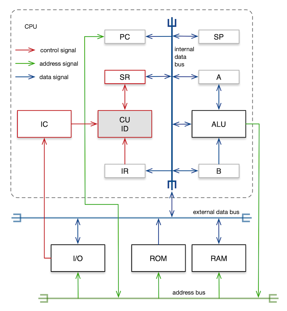
It is often said that the CPU is the brain of the computer. If that were so, the CU is the cerebrum; with the aid of ID, IC, and SR, the CU controls all activities that take place inside the CPU. Many circuitries inside the CPU as well as those in external components are synchronous circuits. These components must be driven by the master clock signal in order for them to operate in synchrony. Timing signals go to every component in the system. To reduce clutter, timing signal paths are not shown in the above diagram. A typical classic 8-bit home computer ran at the clock frequency between 1 and 2 MHz. This clock signal is supplied by an external crystal oscillator.
The CPU chip is plugged into a socket on the motherboard, and the socket pins are connected to clock line, interrupt line, reset line, power line, ground line, address bus lines, and data bus lines. The buses connect the CPU chip to ROM chips, RAM chips, video interface, audio interface, keyboard interface, and other peripherals located around the motherboards. The unidirectional address bus is 16 bits wide, so the CPU can address 64 KB of memory. Address signals travel from the CPU to the address decoders inside the peripherals. The bidirectional data bus is 8 bits wide. Data signals travel in both directions between the CPU and the peripherals. The external data bus is connected to the internal data bus via a tri-state digital buffer. This buffer electrically isolates the internal data bus from the external data bus. It connects the two buses only when the CPU instructs it to do so. And it also controls the I/O data flow direction. The buffer also isolates each peripheral from the external data bus, so that when a peripheral is inactive, it does not interact electrically with the bus. When the CPU wishes to communicate with a peripheral device, the CU causes that device to become active and all other peripherals to become inactive, thereby leaving the data bus for the exclusive use of the CPU and the chosen device. This chain of events constitutes bus arbitration.
The primary function of the CPU is to run programmes. Programmes are sequences of machine instructions. The CPU runs the programme by fetching, decoding, and executing the first instruction, then the next, and the next, and so on. The very procedure executed after the CPU powers up is the reset interrupt service procedure. This procedure, along with other interrupt service procedures are stored in the ROM. When an interrupt occurs during normal operation, the CPU suspends the currently executing procedure, and runs the interrupt service procedure. Once the interrupt has been serviced, the CPU resumes executing the suspended procedure. We shall now examine these operational stages, individually.
fetch
For the CPU to execute an instruction, it must first fetch the instruction from memory. System service procedures and interrupt service procedures are stored in the ROM and user programmes are stored in the RAM. The address of the instruction to be fetched must already be held in the PC. At the start of the fetch stage, the CU transmits the instruction address held in the PC along the address bus. The address decoder of the ROM (or that of the RAM) recognises this address as being one of its own, retrieves the contents of the addressed byte, and transmits the contents along the data bus. The CU knows that the transmitted byte is an instruction, so it loads the instruction into the IR.
decode
The CU now proceeds to the decode stage. The CU instructs the ID to interpret the contents of the IR. The circuitry inside the ID recognises the instruction type: arithmetic operation, logic operation, conditional branch, procedure call, memory access, I/O access, or whatever.
execute
Having decoded the instruction, the CPU enters the execution stage. If the instruction is a read-from-RAM, say one that uses absolute addressing, the CU knows that the instruction comprises three bytes—one byte for the opcode and two bytes for the operand address. The CU uses the operand address to retrieve the addressed byte from RAM, and loads the contents into accumulator A. The ALU can now use the value in accumulator A as an operand. The CU then increments the PC by 3, so the PC now holds the address of the next instruction.
If the instruction is an add operation, the CPU instructs the ALU to add the 8-bit contents of accumulator A and register B, and puts the sum into accumulator A. An addition may generate a carry. A subtraction, on the other hand, may yield a zero or a negative. The CU sets the carry, zero, or negative bit in the SR, depending on the result in accumulator A.
If the instruction is a conditional branch, say one that uses relative addressing and with a loop termination condition i < 10 where i is the loop index, the CU increments the loop index and subtracts 10 therefrom. If the result in accumulator A is not 0, the loop must continue. Then, the CU decrements the PC by the jump distance specified in the branch instruction. At the start of the next fetch stage, the CU will execute the first instruction at the top of the loop, thereby iterating through the loop once more. If the result in accumulator A is 0, however, the CU increments the PC by 2, so the PC now holds the address of the instruction that follows the end of the loop. The CU will fetch that instruction at the start of the next fetch stage.
interrupt
When the CPU receives an interrupt signal from a peripheral, the IC checks if the interrupt is an IRQ or an NMI. If the interrupt is an IRQ, the IC checks if it has sufficient priority to interrupt the currently executing procedure. If the interrupt is an NMI, however, the IC informs the CU to handle the interrupt, immediately.
Before handling an interrupt, the CU finishes the currently executing instruction first, and pushes the current values of the SR and the PC onto the stack. This effectively suspends the currently executing procedure. Next, the CU loads the PC with the address of the interrupt service procedure. The CU knows where to fetch the service procedure’s address, because the address is stored in the interrupt vector table, indexed by the interrupt number. The interrupt vector table is located in ROM at 00000000,00000000 (or, 11111111,11111111, depending on the CPU design). So, if the interrupt number is 1, its service procedure address is stored in the vector table at the following location:
(00000000,00000000 base) + (interrupt number 1) * (2 bytes/address) =
  00000000,00000010 holds low byte of handler address
  00000000,00000011 holds high byte of handler address
Since every address is two bytes in length, the low byte value of the service procedure’s address is at ROM location 00000000,00000010 (decimal $2$) and the high byte value of the address is at ROM location 00000000,00000011 (decimal $3$). The values of these two bytes together form the address of the service procedure for interrupt number 1, and this address is loaded into PC. The CU will execute the first instruction of the handler procedure, starting at the next fetch stage.
Upon reaching the interrupt return instruction at the end of the handler procedure, the CU pops the saved PC and SR values off the stack and loads the saved PC value into the PC and saved SR value into the SR, thereby restoring the suspended procedure’s state. The suspended procedure resumes execution at the start of the next fetch stage.
CONCLUSION
I explained in this article how a computer is built, how it boots up, how it executes instructions, how it performs simple calculations, how these calculations when combined exhibit behaviours as complex as playing chess. My main goal here was to give software developers a better understanding of how the computer hardware executes programmes, with the hope that this low-level understanding may make them more mechanically sympathetic programmers. This hardware execution model I presented also sheds light on the inner workings of virtualisation technologies, hardware emulators, virtual machines, and microcontrollers.
As much as possible, I avoided descending into the low-level details like radiation shielding, clock signal phases, clock skew, signal degradation during bus transfer, serial and parallel I/O protocols, power regulation, heat dissipation, circuit layout, chip fabrication, etc. I also shunned modern, advanced topics like pipelining, branch prediction, vector processing, SIMD, VLIW, multi-core processors, on-chip instruction and data caches, on-chip high-speed buses, NUMA, etc. Those interested in modern processors and microcontrollers should read textbooks like Computer Architecture: A Quantitative Approach and The Designer’s Guide to the Cortex-M Processor Family: A Tutorial Approach.
RESOURCES
- 6502.org
- This site is the most comprehensive repository of 6502 resources. Its books page lists many of the classic publications on general assembly programming, as well as those that focus on the 6502.
- The Visual 6502
- This web application visualises a 6502, as it executes code. You can run the CPU at full speed or single step it. The single-stepping execution mode is particularly enlightening.
- KIM-1 Simulator
- The KIM-1 was the most popular trainer for the 6502. Many people learn microprocessor programming on trainers, back in the day. This web application simulates that learning experience.